01
Rare-earth composition & ratios
Change host and dopant combinations to shift excitation pathways, emission wavelengths, intensity ratios and interaction between energy levels.
Intelligent Material connects the physical world with the digital world. Our inert rare-earth crystals convert energy into measurable information. We engineer the crystal itself, changing how it interacts with light, energy, magnetic fields and its surrounding environment.
The most powerful use of Intelligent Material is becoming part of the product itself. Once the crystal is inside a polymer, coating, ink, oil, fiber, biological assay or other compatible system, the product carries a persistent engineered response from the moment it is made.
We can encode information into composition, structure, wavelength response, lifetime, excitation dependence, magnetic behavior and core/shell interactions.
The result is a material that can convert energy, carry information and remain physically connected to the thing being measured, authenticated or controlled.
IMS treats each crystal as a multidimensional information carrier whose response can be engineered for a specific purpose.
Change host and dopant combinations to shift excitation pathways, emission wavelengths, intensity ratios and interaction between energy levels.
Control particle dimensions, crystal facets and uniformity to influence optical behavior, surface interactions, processing and self-assembly.
Engineer rise, decay, persistence and lifetime behavior so time itself becomes another dimension of the material identity.
Combine optical and magnetic behavior to create materials that can be identified optically while responding to magnetic fields or separation methods.
Separate, couple or enhance functions across nanoscale interfaces, including energy transfer, isolation, surface chemistry and plasmonic effects.
Vary excitation power density and measure how emission responds. The intensity-dependent response curve becomes another way to identify the material.
Rare-earth ions occupy discrete electronic energy states. By choosing the host, dopants and concentrations, we engineer which wavelengths are absorbed and which wavelengths are emitted.
Two or more lower-energy excitation events can populate higher excited states. The material can then emit a shorter-wavelength photon, allowing invisible near-infrared excitation to produce visible light.
A higher-energy photon is absorbed and the excited ion relaxes before emitting at a longer wavelength. We can engineer this response across UV, visible and infrared regions.
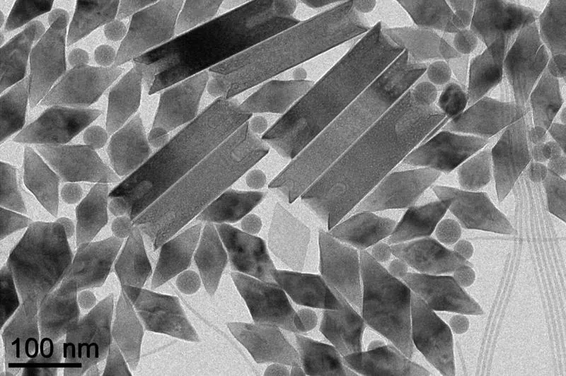
A counterfeiter can match a color. Matching the crystal is another story. Intelligent Material grows the same rare-earth emitter as rods, hexagonal plates, diamonds or spheres, and decides whether to build in ytterbium, the antenna that soaks up 980 nm light and hands it to the emitter. Spin the lock, then watch the reader check every layer.
Illustration. Laser responses, polarization patterns and rise times are simplified for display, Nd³⁺ infrared emission is shown in false color, and timing is slowed for the eye. Not a validated panel.
Rare-earth crystals are not the same in every direction. A rod glows brightest when the reader's polarizer lines up with its long axis, a flat hexagonal plate prefers the crossing direction, a faceted diamond answers in four lobes, and a sphere looks the same from every angle. Turn a polarizer and the shape shows up in the signal, with no microscope.
Ytterbium absorbs 980 nm light roughly ten times better than erbium does, then hands the energy to its emitter neighbor. Leave it out and the very same Er³⁺ crystal barely notices 980 nm and needs 1550 nm instead. How much Yb is built in also sets how fast the glow rises, a timing signature a copy has to match.
Reader logic: U.S. Patent 11,435,228 B2 ↗Everything above was one solid crystal. Grow layers around it, a core and three shells, each with its own ingredient, and let energy hop from layer to layer. Every layer multiplies the choices. That is where the combinations go through the roof.
Build a crystal layer by layer. The reader does not just see a color: it watches how the light rises and decays over time, and how the answer changes as the laser power goes up. Layers that pass energy to each other leave their own fingerprint in both. Pick a recipe, or let the mint make a fresh one.
Illustration. Energy-transfer efficiencies, power slopes, lifetimes and spectra come from a simplified model of layered upconverting crystals, not measured data; real recipes are designed and verified in the lab. Plots are drawn in the style of time-resolved spectra, with intensity mapped to color.
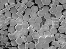
Most taggants are solid-state phosphors: fired, crushed and milled into jagged grains several microns across, no two alike. Intelligent Material grows every particle to the same size and shape. Same field of view, same laser spot scanning across both:
Disordered, irregular, microscopic.
Uniform, controllable morphology, nanoscopic.
The code space · scroll to turn the dials
Every crystal is a combination lock: each design choice is another dial. Scroll down and watch the lock gain dials, first inside one crystal, then in the shells grown around it, and finally when a customer mixes several crystals into one mark. Each new dial multiplies the number of codes.
Pick the rare-earth emitter, the crystal shape and how much ytterbium antenna to build in. The reader checks all three: color, polarization and how fast the glow rises.
6 × 4 × 3 = 72 different crystals.
Change the size or the dopant level and the glow fades at a different speed. Seven lifetimes the reader can tell apart add a fourth dial to the same crystal.
72 × 7 = 504 crystals.
Grow a core and three shells around it, each with its own ingredient, amount and thickness, and let energy hop from layer to layer. Every shell is a new dial with 111 positions. The lock gets much bigger.
111⁴ layer recipes × 4 shapes ≈ 607 million single-crystal codes.
Now open the whole library of shelled crystals and blend up to twenty of them in one ink. The lock becomes a galaxy of locks: more codes than there are atoms in the observable universe, by a factor of about 1077.
Illustration. Counts assume every combination can be told apart by the reader; real code books are designed with margins between codes.
Where the code goes
The crystals are inert, uniform and smaller than a wavelength of light, so they disperse into the materials manufacturers already use, at parts per million to thousandths of a percent. The code is made into the product, not stuck on afterwards.
The most common home for the code. The crystals are smaller than the nozzles and pigments the ink already carries.
Compounded into masterbatch pellets, so every molded or extruded part carries the code from the first shot.
Added with a spinning ingredient at about 5 ppm in the finished fiber, and readable all the way to the finished garment.
Blended into the melt to prove origin, even after the metal comes back as scrap, or carried in coatings on the surface.
Coated crystals disperse in oils and fuels to mark the product, or are injected to trace where fluid flows underground.
In the adhesive that seals a package, so opening it leaves a measurable trace. Surgical packaging uses about 0.001%.
Anything that can hold a fine, inert powder is a candidate: paper, glass, ceramics, rubber, wax, paints, even cement. We test the crystal in your own material first.
Start with a sample →*Any food, cosmetic or medical use requires its own safety and regulatory review. Loadings shown are typical examples.
The Crystal Lab, run by Intelligent Material Solutions, is where partners design a crystal and see what it does: choose the host, the rare-earth ions and the lasers, then read the color, spectrum and timing it produces.
Define the physical and chemical environment around the active ions.
Select activators and sensitizers and tune their concentrations.
UV, visible, 808, 940, 980, 1550 nm and other optical inputs.
Spectrum, lifetime, power-density response, magnetics and core/shell behavior.
Christopher B. Murray is an inventor on the IMS / University of Pennsylvania uniform-crystal patent family. He was also first author, with David Norris and Moungi Bawendi, on the landmark 1993 paper describing a controlled synthesis of nearly monodisperse semiconductor nanocrystals.
The 2023 Nobel Prize in Chemistry recognized Moungi Bawendi, Louis Brus and Aleksey Yekimov for the discovery and synthesis of quantum dots. The Nobel background specifically identifies Bawendi's 1993 advance in producing high-quality quantum dots with controlled size. IMS's work applies the same broader lesson to a different materials platform: precise control of nanoscale composition, size and architecture creates precise control of material behavior.
Synthesis and characterization of nearly monodisperse CdE semiconductor nanocrystallites.
Read the paper · 2023 Nobel Prize context
IMS / Penn patentMorphologically and size uniform monodisperse particles and their shape-directed self-assembly. Inventors include Howard Bell, Joshua Collins, Xingchen Ye and Christopher Bruce Murray.
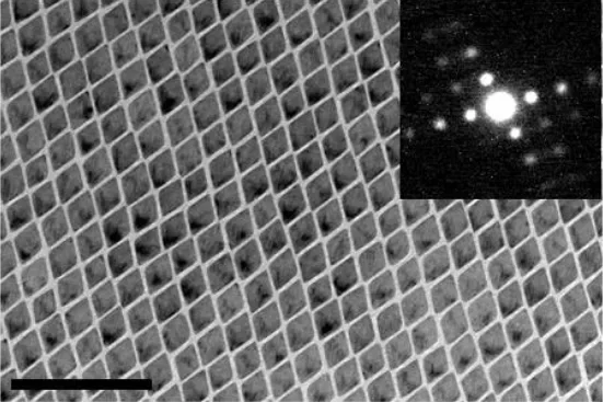
Intelligent Material grew out of work with Christopher Murray's group at the University of Pennsylvania. Two peer-reviewed papers, in PNAS and Nature Chemistry, both co-authored by Joshua E. Collins of Intelligent Material Solutions, show the core idea: grow every crystal to the same size and shape, and they arrange themselves into near-perfect patterns, with no one placing them.
In a single flask, the team grew upconverting crystals of sodium yttrium fluoride, the same host used in many IMS crystals, doped with ytterbium and erbium for green light or ytterbium and thulium for blue. Changing just the reaction time and the ratio of sodium to rare earth turned spheres into rods, hexagonal prisms and flat plates.
Drawn by IMS from the paper's findings. Plates with only shape to go on pack one way; when unlike edges attract more strongly (gold), rows flip and alternate. That alternating pattern is what the electron microscope showed, and what the computer simulations predicted.
The 2013 paper moved to flat rare-earth fluoride plates, from lanthanum through holmium, shaped as rhombs and stretched hexagons. Pure geometry predicts one packing. The real plates often chose another.
The reason is the coating. Each crystal wears a fringe of oleic acid, and computer models showed it grips one kind of edge almost six times harder than another: about 0.70 versus 0.12 electron-volts. Edges that are "stickier" than others, or patchy, compete with shape to decide the pattern.
All illustrations drawn by IMS from the findings of Ye et al., PNAS 107, 22430–22435 (2010) and Ye et al., Nature Chemistry 5, 466–473 (2013). Read the papers for the original data and micrographs.
The portfolio spans uniform particles and assemblies, temporal authentication, rare-earth materials in articles and systems for identifying Intelligent Material from its engineered emission response.
Monodisperse particles and shape-directed self-assembly developed with the University of Pennsylvania.
Related claims involving up- and down-converting particles, polyhedral morphology and organized superlattices.
Authentication using engineered temporal characteristics of the emission response.
IR-blocking inks incorporating rare-earth Intelligent Material for article and transaction-card authentication.
Methods and systems for identifying Intelligent Material from changes in emission response under controlled illumination.
Start with the material itself. NovaVera and IMS define the excitation, emission, timing, power-density, magnetic and structural response your application needs, then supply it in the ink, plastic, fiber or coating you already use.